| CPC H10K 59/1315 (2023.02) [H10K 59/124 (2023.02); H10K 59/131 (2023.02); H01L 27/124 (2013.01); H10K 50/841 (2023.02); H10K 50/844 (2023.02); H10K 50/8426 (2023.02); H10K 50/87 (2023.02); H10K 59/1213 (2023.02)] | 14 Claims |
|
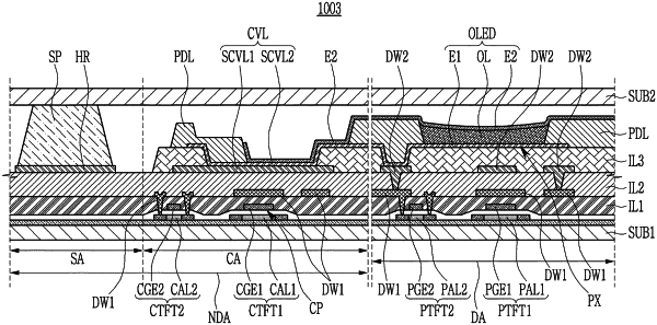
1. An organic light emitting diode display comprising:
a substrate including a display area and a non-display area adjacent to the display area;
a pixel thin film transistor positioned in the display area of the substrate;
a first conductive layer positioned over the pixel thin film transistor;
a second conductive layer positioned over the first conductive layer;
an organic light emitting element positioned over the second conductive layer and electrically connected to the pixel thin film transistor through the first conductive layer and the second conductive layer;
a circuit unit positioned in the non-display area of the substrate and including a circuit thin film transistor electrically connected to the pixel thin film transistor; and
a common power supply line overlapping at least part of the circuit unit, electrically connected to the organic light emitting element, and formed on a same layer as the second conductive layer,
wherein the first conductive layer is connected to the pixel thin film transistor and the second conductive layer,
wherein the non-display area includes:
a circuit area adjacent to the display area and including the circuit unit and the common power supply line; and
a sealing area adjacent to the circuit area, the organic light emitting diode display further comprising a sealing part positioned in the sealing area and a heat reflection part in contact with the sealing part between the sealing part and the substrate,
wherein the heat reflection part is isolated from the common power supply line or the circuit unit, and
wherein the heat reflection part is positioned over the first conductive layer and on a same layer as the second conductive layer.
|