| CPC H10K 50/844 (2023.02) [H10K 59/122 (2023.02); H10K 59/40 (2023.02); H10K 71/00 (2023.02); H10K 59/1201 (2023.02)] | 4 Claims |
|
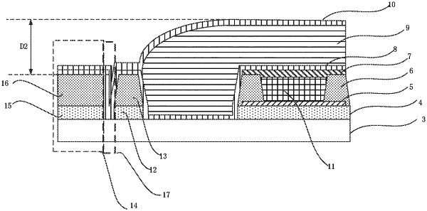
1. A method of manufacturing a display panel, wherein the display panel comprises a display area and a hole forming area, the display area surrounds the hole forming area; the display area comprises: a thin film transistor array layer on a base substrate, a planarization layer covering the thin film transistor array layer, and a pixel defining layer on the planarization layer;
the method comprises:
forming a second organic material sub-layer in the hole forming area and the planarization layer in the display area through a single patterning process;
forming a first organic material sub-layer in the hole forming area and the pixel defining layer in the display area through a single patterning process,
wherein the first organic material sub-layer and the second organic material sub-layer form an organic material layer,
wherein the forming the second organic material sub-layer in the hole forming area and the planarization layer in the display area through the single patterning process comprises:
forming a photosensitive organic material layer;
exposing the photosensitive organic material layer by using a gray-tone mask, wherein the gray-tone mask comprises a partially light-transmitting pattern corresponding to the display area and an opaque pattern corresponding to the hole forming area;
performing a development process to form the second organic material sublayer in the hole forming area and the planarization layer in the display area, wherein a thickness of the second organic material sub-layer is greater than a thickness of the planarization layer in the display area.
|