| CPC H10B 51/20 (2023.02) [H01L 21/02565 (2013.01); H01L 29/24 (2013.01); H10B 51/30 (2023.02)] | 20 Claims |
|
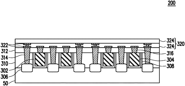
1. A device, comprising:
a dielectric layer having a first surface and a second surface opposite to the first surface;
a conductive layer disposed on the first surface of the dielectric layer;
electrode layers disposed on the second surface of the dielectric layer; and
an oxide semiconductor layer disposed in between the second surface of the dielectric layer and the electrode layers, wherein the oxide semiconductor layer comprises a first sub-layer including a material represented by formula 1, and a second sub-layer including the material represented by formula 1, wherein the first sub-layer is a crystalline layer and the second sub-layer is an amorphous layer:
InxSnyTizMmOn [formula 1]
wherein in formula 1, 0<x<1, 0≤y<1, 0<z<1, 0<m<1, 0<n<1, and M represents at least one metal.
|