| CPC H10B 43/27 (2023.02) [G11C 16/08 (2013.01); H10B 41/10 (2023.02); H10B 41/27 (2023.02); H10B 41/35 (2023.02); H10B 43/10 (2023.02); H10B 43/35 (2023.02)] | 20 Claims |
|
1. A method of forming a microelectronic device, comprising:
forming a microelectronic device structure, the microelectronic device structure comprising:
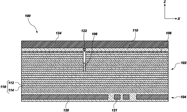
a stack structure comprising insulative structures and additional insulative structures vertically alternating with the insulative structures;
a dielectric structure vertically extending partially through the stack structure; and
a dielectric material vertically overlying and horizontally extending across the stack structure and the dielectric structure;
removing portions of at least the dielectric material and the dielectric structure to form a trench vertically overlying and at least partially horizontally overlapping a remaining portion of the dielectric structure; and
substantially filling the trench with additional dielectric material.
|