| CPC H10B 12/315 (2023.02) [H10B 12/482 (2023.02); H10B 12/488 (2023.02)] | 18 Claims |
|
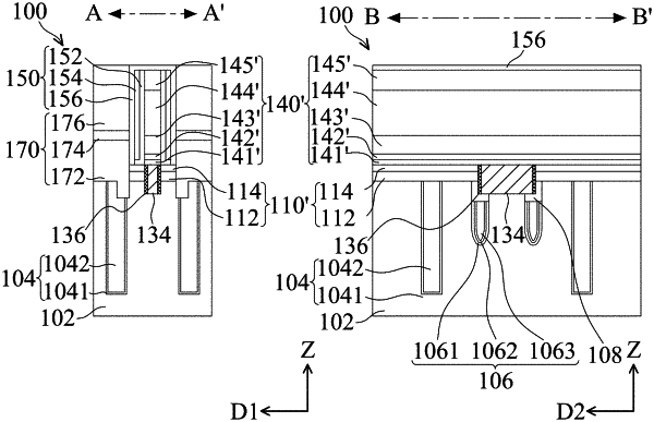
1. A method for forming a semiconductor memory structure, comprising:
providing a semiconductor substrate, wherein a pair of word lines is embedded in an active region of the semiconductor substrate and extends in a first direction;
forming a hard mask layer on the semiconductor substrate;
forming a contact opening corresponding to the pair of word lines through the hard mask layer and a portion of the semiconductor substrate;
forming a pair of spacers on sidewalls of the contact opening;
filling the contact opening with a conductive material to form a contact;
planarizing a portion of the hard mask layer and the conductive material to be coplanar after the step of filling the conductive material, wherein a remaining of the conductive material acts as the contact and a remaining of the hard mask layer acts as a cap layer;
forming a bit line directly above the contact and the pair of spacers after the step of planarizing, wherein the bit line extends in a second direction that is perpendicular to the first direction; and
forming a dielectric liner on sidewalls of the bit line.
|