| CPC H10B 12/315 (2023.02) [H10B 12/395 (2023.02); H10B 12/50 (2023.02)] | 20 Claims |
|
13. A semiconductor memory device, comprising:
a peripheral circuit structure comprising a plurality of peripheral circuits on a semiconductor substrate and a lower insulating layer covering the plurality of peripheral circuits;
a plurality of bit lines extended in a first direction on the peripheral circuit structure;
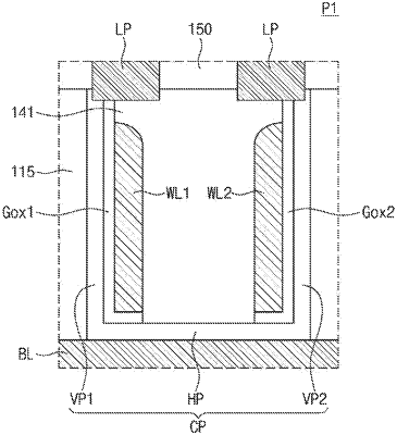
a first insulating pattern defining a trench, the first insulating pattern crossing the plurality of bit lines and extending in a second direction;
a plurality of channel patterns provided in the trench and spaced apart from each other in the second direction, each of the plurality of channel patterns comprising a first vertical portion and a second vertical portion facing each other and a horizontal portion connecting the first vertical portion with the second vertical portion;
a first word line and a second word line provided on the horizontal portion of each of the plurality of channel patterns, the first word line and the second word line extending in the second direction, the first word line being adjacent to the first vertical portion of each of the plurality of channel patterns, the second word line being adjacent to the second vertical portion of each of the plurality of channel patterns;
for each of the plurality of channel patterns, a gate insulating pattern extending in the second direction disposed between the channel pattern and the first word line and between the channel pattern and the second word line;
a second insulating pattern covering the first word line and the second word line in the trench;
a plurality of first data storage patterns disposed on respective first vertical portions of the plurality of channel patterns; and
a plurality of second data storage patterns disposed on respective second vertical portions of the plurality of channel patterns,
wherein the first direction and the second direction are substantially parallel to a top surface of the semiconductor substrate.
|