| CPC H05K 1/184 (2013.01) [H05K 1/111 (2013.01); H05K 1/113 (2013.01); H05K 1/16 (2013.01); H05K 1/162 (2013.01); H05K 1/165 (2013.01); H05K 1/167 (2013.01); H05K 1/183 (2013.01); H05K 2201/0305 (2013.01); H05K 2201/09072 (2013.01); H05K 2201/10454 (2013.01)] | 14 Claims |
|
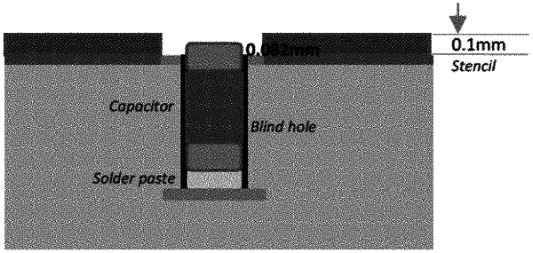
1. A printed circuit board (PCB) comprising:
a blind via in a layer of the PCB, the layer of the PCB having an uppermost surface;
a discrete component vertically embedded within the blind via;
a solder paste pad on the discrete component, the solder paste pad extending laterally beyond the blind via, wherein a portion of the solder paste pad is vertically overlapping with the uppermost surface of the layer of the PCB; and
a stencil on the uppermost surface of the layer of the PCB, the stencil laterally surrounding and in lateral contact with the solder paste pad, wherein the discrete component is vertically embedded under a ball grid array coupling the PCB to an integrated circuit (IC) package, and wherein a solder ball of the ball grid array is vertically over and coupled to the discrete component by the solder paste pad.
|