| CPC H05K 1/14 (2013.01) [H05K 1/0215 (2013.01); H05K 1/0218 (2013.01); H05K 1/117 (2013.01); H05K 1/144 (2013.01); H05K 2201/042 (2013.01); H05K 2201/10378 (2013.01); H05K 2201/2018 (2013.01)] | 16 Claims |
|
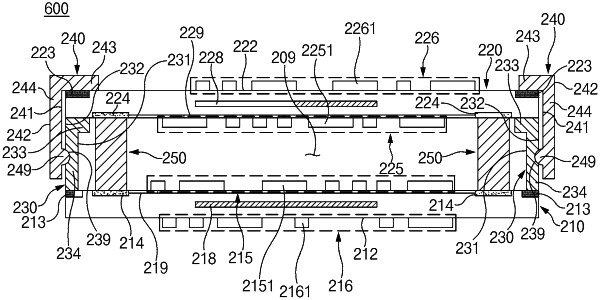
1. An electronic device comprising:
a first substrate on which a first electrical element and a first conductive structure, which is configured to surround the first electrical element, are disposed;
a second substrate on which a second electrical element and a second conductive structure, which is separably connected to the first conductive structure, are disposed; and
a connector which is disposed between the first substrate and the second substrate and electrically connects the first electrical element to the second electrical element,
wherein the first substrate comprises a first surface on which the first conductive structure is disposed and a second surface opposite to the first surface,
wherein the second substrate comprises a third surface facing the first surface and a fourth surface opposite to the third surface,
wherein the first conductive structure is in contact with a partial area of the third surface of the second substrate, and the second conductive structure extends from at least a portion of the fourth surface of the second substrate toward the first surface of the first substrate,
wherein first recess and protrusion structures corresponding to each other are provided in the first surface of the first substrate and one surface of the first conductive structure that are in contact with each other,
wherein second recess and protrusion structures corresponding to each other are provided in the fourth surface of the second substrate and one surface of the second conductive structure that are in contact with each other, and
wherein the first recess and protrusion structures fix the first conductive structure to the first substrate, and the second recess and protrusion structures fix the second conductive structure to the second substrate.
|