| CPC H04B 10/40 (2013.01) [H04B 1/12 (2013.01); H04B 10/503 (2013.01); H04B 10/548 (2013.01); H04L 25/03343 (2013.01)] | 12 Claims |
|
1. A high-speed optical transceiver integrated chip drive circuit with phase delay compensation function, which comprises a transmitting/sending end drive circuit and a receiving end drive circuit, the transmitting end drive circuit is used to drive a laser device to emit light for transmitting signals and the receiving end drive circuit is used to optimize a signal degradation caused by the signal transmission by the transmitter end drive circuit to the laser device through a transmission backplane; characterized in that: comprising: a long code phase lead adjustment circuit provided on a main channel of the transmitter end drive circuit; a long code phase lag adjustment circuit provided on a main channel of the receiving end drive circuit;
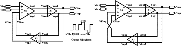
the long code phase lead adjustment circuit comprises an operational amplifier A0, an operational amplifier A1 and an operational amplifier A2,
a non-inverting input terminal Vinp and an inverting input terminal Vinn of the operational amplifier A0 are used to receive external input electrical signals;
an inverting output terminal Von0 of the operational amplifier A0 is connected to a non-inverting input terminal Vinp1 of the operational amplifier A1;
a non-inverting output terminal Vop0 of the operational amplifier A0 is connected to an inverting input terminal Vinn1 of the operational amplifier A1;
an inverting output terminal Von1 of the operational amplifier A1 is simultaneously connected to an output port of the drive circuit Von and an inverting input terminal Vinn2 of the operational amplifier A2;
a non-inverting output terminal Vop1 of the operational amplifier A1 is simultaneously connected to an output port of the drive circuit Vop and a non-inverting input terminal Vinp2 of the operational amplifier A2;
an inverting output terminal Von2 of the operational amplifier A2 is connected to an non-inverting input terminal VFinp of the operational amplifier A0, and a non-inverting output terminal Vop2 of the operational amplifier A2 is connected to an inverting input terminal VFinn of the operational amplifier A0;
the long code phase lag adjustment circuit comprises an operational amplifier A0, an operational amplifier A1 and an operational amplifier A2,
a non-inverting input terminal Vinp and an inverting input terminal Vinn of the operational amplifier A0 are used to receive external input electrical signals;
an inverting output terminal Von0 of the operational amplifier A0 is connected to a non-inverting input terminal Vinp1 of the operational amplifier A1;
a non-inverting output terminal Vop0 of the operational amplifier A0 is connected to an inverting input terminal Vinn1 of the operational amplifier A1;
an inverting output terminal Von1 of the operational amplifier A1 is simultaneously connected to an output port of the drive circuit Von and an inverting input terminal Vinn2 of the operational amplifier A2;
a non-inverting output terminal Vop1 of the operational amplifier A1 is simultaneously connected to an output port of the drive circuit Vop and a non-inverting input terminal Vinp2 of the operational amplifier A2;
wherein an inverting output terminal Von2 of the operational amplifier A2 is connected to an inverting input terminal VFinn of the operational amplifier A0 while a non-inverting output terminal Vop2 of the operational amplifier A2 is connected to a non-inverting input terminal VFinp of the operational amplifier A0; or an inverting output terminal Von2 of the operational amplifier A2 is connected to a non-inverting input terminal VFinp of the operational amplifier A0, and a non-inverting output terminal Vop2 of the operational amplifier A2 is connected to an inverting input terminal VFinn of the operational amplifier A0.
|