| CPC H03K 19/01714 (2013.01) [H01L 27/0922 (2013.01); H01L 29/0665 (2013.01); H03K 19/0013 (2013.01)] | 10 Claims |
|
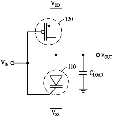
1. A logic-in-memory inverter comprising:
a metal oxide semiconductor field-effect transistor; and
a feedback field-effect transistor in which a drain region of a nanostructure is connected in series to a drain region of the metal oxide semiconductor field-effect transistor,
wherein the logic-in-memory inverter performs a logical operation based on an output voltage VOUT that changes depending on a level of an input voltage VIN that is input to a gate electrode of the feedback field-effect transistor and a gate electrode of the metal oxide semiconductor field-effect transistor while a source voltage VSS is input to a source region of the nanostructure and a drain voltage VDD is input to a source region of the metal oxide semiconductor field-effect transistor.
|