US 11,695,414 B2
Multi-gated I/O system, semiconductor device including and method for generating gating signals for same
Shao-Te Wu, Hsinchu (TW); Chia-Jung Chang, Hsinchu (TW); and Shih-Peng Chang, Hsinchu (TW)
Assigned to TAIWAN SEMICONDUCTOR MANUFACTURING COMPANY, LTD., Hsinchu (TW)
Filed by TAIWAN SEMICONDUCTOR MANUFACTURING COMPANY, LTD., Hsinchu (TW)
Filed on Dec. 8, 2021, as Appl. No. 17/544,953.
Application 17/544,953 is a continuation of application No. 17/028,727, filed on Sep. 22, 2020, granted, now 11,201,618.
Claims priority of provisional application 62/990,298, filed on Mar. 16, 2020.
Prior Publication US 2022/0103171 A1, Mar. 31, 2022
This patent is subject to a terminal disclaimer.
Int. Cl. H03K 3/012 (2006.01); H03K 5/00 (2006.01); H03K 17/22 (2006.01); H03K 19/003 (2006.01); H03K 17/687 (2006.01); G06F 30/392 (2020.01); H03K 19/0175 (2006.01)
CPC H03K 17/6872 (2013.01) [G06F 30/392 (2020.01); H03K 19/017509 (2013.01)] 20 Claims
OG exemplary drawing
 
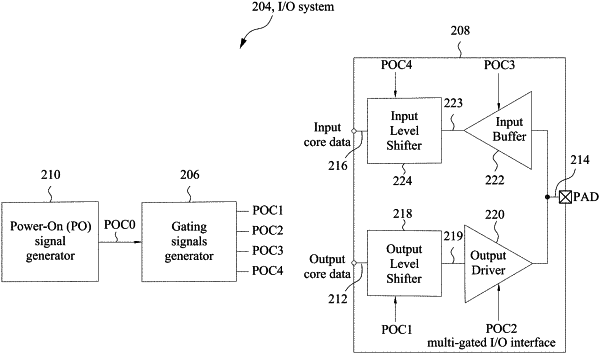
1. A method of generating multiple gating signals for a multi-gated input/output (I/O) system that includes an output level shifter and an output driver which are coupled in series between an output node of a core circuit and an external terminal of a corresponding system, the method comprising:
generating first and second gating signals having corresponding first and second waveforms, the first and second waveforms being free from relating as waveform-inversions of each other, and the first waveform transitioning from a non-enabling state to an enabling state before the second waveform transitions from the non-enabling state to the enabling state;
receiving the first gating signal at the output level shifter; and
receiving the second gating signal at the output driver.