| CPC H03K 3/0375 (2013.01) [H03K 3/57 (2013.01); G11C 11/4076 (2013.01); G11C 11/4093 (2013.01)] | 14 Claims |
|
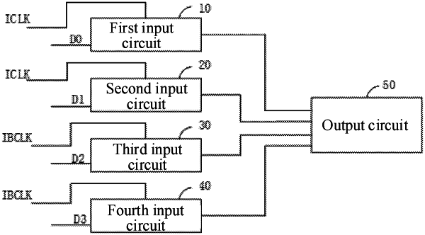
1. A data synthesizer, comprising:
a first input circuit, configured to latch first data under control of a first latch clock signal;
a second input circuit, configured to latch second data under the control of the first latch clock signal, wherein a phase of the first data is the same as a phase of the second data; and
an output circuit, connected to the first input circuit and the second input circuit, and configured to output the first data and the second data in sequence,
wherein the output circuit comprises:
a first switch circuit, having a first terminal, a second terminal and a control terminal, wherein the first terminal of the first switch circuit is connected to an output terminal of the first input circuit, the second terminal of the first switch circuit is taken as an output terminal of the output circuit, the control terminal of the first switch circuit is configured to receive a first output clock signal, and the first switch circuit is configured to output, through the second terminal of the first switch circuit, the first data under control of the first output clock signal; and
a second switch circuit, having a first terminal, a second terminal and a control terminal, wherein the first terminal of the second switch circuit is connected to an output terminal of the second input circuit, the second terminal of the second switch circuit is connected to the second terminal of the first switch circuit, the control terminal of the second switch circuit is configured to receive a second output clock signal, and the second switch circuit is configured to output, through the second terminal of the second switch circuit, the second data under control of the second output clock signal.
|