US 11,695,220 B2
Array antenna
Jae Yeong Kim, Suwon-si (KR); Ji Hyung Jung, Suwon-si (KR); Chin Mo Kim, Suwon-si (KR); Sung Nam Cho, Suwon-si (KR); and Sung Yong An, Suwon-si (KR)
Assigned to Samsung Electro-Mechanics Co., Ltd., Suwon-si (KR)
Filed by Samsung Electro-Mechanics Co., Ltd., Suwon-si (KR)
Filed on Apr. 5, 2022, as Appl. No. 17/713,453.
Application 17/713,453 is a continuation of application No. 16/732,661, filed on Jan. 2, 2020, granted, now 11,322,856.
Claims priority of application No. 10-2019-0109396 (KR), filed on Sep. 4, 2019.
Prior Publication US 2022/0231430 A1, Jul. 21, 2022
This patent is subject to a terminal disclaimer.
Int. Cl. H01Q 21/06 (2006.01); H01Q 1/52 (2006.01); H01Q 1/22 (2006.01); H01Q 1/38 (2006.01)
CPC H01Q 21/065 (2013.01) [H01Q 1/2283 (2013.01); H01Q 1/38 (2013.01); H01Q 1/526 (2013.01)] 17 Claims
OG exemplary drawing
 
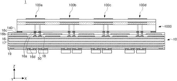
1. An array antenna comprising:
an antenna substrate comprising a first ceramic member, an insertion member, and a second ceramic member stack;
antenna pattern portions arranged on the antenna substrate in an array form and including patches disposed on the first ceramic member and between the first ceramic member and the insertion member; and
shielding vias disposed inside the antenna substrate and extending in a thickness direction of the antenna substrate,
wherein the plurality of shielding vias are disposed in thickness areas of the antenna substrate corresponding to the antenna pattern portions.