| CPC H01L 33/0095 (2013.01) [H01L 25/0753 (2013.01); H01L 33/0093 (2020.05)] | 20 Claims |
|
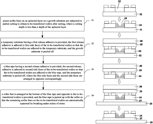
1. A transfer method, comprising:
performing partial cutting on preset scribe lines on an epitaxial layer on a growth substrate to obtain to-be-transferred wafers after cutting, wherein a cutting depth is less than a depth of the epitaxial layer;
providing a temporary substrate having a first release adhesive, adhering the first release adhesive to first side faces of the to-be-transferred wafers so as to adhere the to-be-transferred wafers to the temporary substrate, and peeling off the growth substrate;
providing a blue tape having a second release adhesive, adhering the second release adhesive to second side faces of the to-be-transferred wafers so as to adhere the to-be-transferred wafers to the blue tape, and peeling off the temporary substrate, wherein the first side faces and the second side faces are arranged in opposite correspondingly; and
providing a roller that is arranged at the bottom of the blue tape and opposite to the to-be-transferred wafers, and jacking up the blue tape with the roller so that remaining scribe lines on the to-be-transferred wafers are separated by breaking under action of stress.
|