| CPC H01L 31/022441 (2013.01) [H01L 31/028 (2013.01); H01L 31/02363 (2013.01); H01L 31/022466 (2013.01); H01L 31/0682 (2013.01)] | 27 Claims |
|
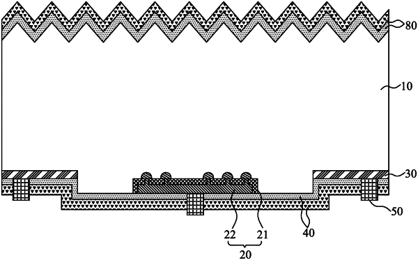
1. A back contact structure of a solar cell, the back contact structure comprising:
a silicon substrate, the silicon substrate comprising a back surface comprising a plurality of recesses disposed at intervals such that a protrusion is formed between two adjacent recesses of the plurality of recesses;
a plurality of first conductive regions and a plurality of second conductive regions disposed alternately in the plurality of recesses, wherein each first conductive region comprises a first dielectric layer and a first doped region which are disposed successively in the plurality of recesses, and each second conductive region consists of a second doped region;
a second dielectric layer, wherein the second dielectric layer is at least one in number; and
a conductive layer disposed on the plurality of first conductive regions and the plurality of second conductive regions;
wherein
a thickness of the plurality of first conductive regions is less than a depth of the plurality of recesses, and the first dielectric layer and the first doped region are enclosed inside the plurality of recesses;
the second dielectric layer comprises a first portion, a second portion, and a third portion;
the first portion is disposed on and covers a top surface of the first doped region, and the first portion is constrained on the plurality of recesses where the plurality of first conductive regions is disposed;
the second portion is disposed on and covers a side wall of the plurality of recesses where the plurality of second conductive regions is disposed and a top surface of the second conductive region, and the second portion is constrained inside the plurality of recesses where the plurality of second conductive regions is disposed; and
the third portion is disposed between the first portion and the second portion and is constrained on the protrusion.
|