US 11,695,076 B2
FET with wrap-around silicide and fabrication methods thereof
Pei-Hsun Wang, Kaohsiung (TW); Chih-Chao Chou, Hsinchu (TW); Shih-Cheng Chen, New Taipei (TW); Jung-Hung Chang, Changhua County (TW); Jui-Chien Huang, Hsinchu (TW); Chun-Hsiung Lin, Hsinchu County (TW); and Chih-Hao Wang, Hsinchu County (TW)
Assigned to TAIWAN SEMICONDUCTOR MANUFACTURING CO., LTD., Hsinchu (TW)
Filed by Taiwan Semiconductor Manufacturing Co., Ltd., Hsinchu (TW)
Filed on Mar. 5, 2021, as Appl. No. 17/193,732.
Application 17/193,732 is a division of application No. 16/582,547, filed on Sep. 25, 2019, granted, now 10,944,009.
Claims priority of provisional application 62/753,466, filed on Oct. 31, 2018.
Prior Publication US 2021/0193842 A1, Jun. 24, 2021
Int. Cl. H01L 29/786 (2006.01); H01L 29/06 (2006.01); H01L 29/423 (2006.01); H01L 29/45 (2006.01); H01L 29/66 (2006.01); H01L 21/02 (2006.01); H01L 21/285 (2006.01)
CPC H01L 29/78618 (2013.01) [H01L 21/02532 (2013.01); H01L 21/02603 (2013.01); H01L 21/28518 (2013.01); H01L 29/0653 (2013.01); H01L 29/0673 (2013.01); H01L 29/42392 (2013.01); H01L 29/45 (2013.01); H01L 29/66545 (2013.01); H01L 29/66742 (2013.01); H01L 29/78684 (2013.01); H01L 29/78696 (2013.01)] 20 Claims
OG exemplary drawing
 
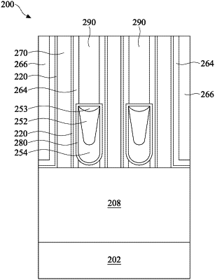
1. A semiconductor device, comprising:
a semiconductor fin disposed over a substrate;
an isolation structure at least partially surrounding the semiconductor fin;
a source/drain (S/D) feature disposed over the semiconductor fin, wherein an extended portion of the S/D feature extends over the isolation structure; and
a silicide layer disposed over the S/D feature, wherein the silicide layer fully wraps around the extended portion of the S/D feature when viewed in a cross-section cut vertically along a length of the semiconductor fin.