| CPC H01L 29/78391 (2014.09) [G11C 11/223 (2013.01); G11C 11/2255 (2013.01); G11C 11/2257 (2013.01); H01L 29/04 (2013.01); H01L 29/24 (2013.01); H01L 29/66969 (2013.01); H01L 29/7869 (2013.01); H10B 51/10 (2023.02); H10B 51/20 (2023.02); H10B 51/30 (2023.02)] | 20 Claims |

|
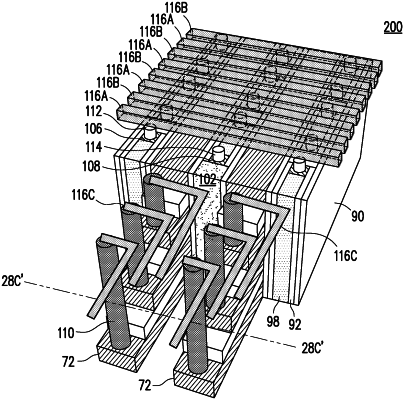
1. A memory cell comprising:
a transistor over a semiconductor substrate, the transistor comprising:
a ferroelectric (FE) material directly contacting a word line, the FE material being a hafnium-comprising compound, and the hafnium-comprising compound comprising a rare earth metal, wherein the word line is one of a plurality of vertically stacked word lines, and wherein the FE material directly contacts a respective sidewall of each of the plurality of vertically stacked word lines; and
an oxide semiconductor (OS) layer contacting a source line and a bit line, wherein the FE material is disposed between the OS layer and the word line, and wherein the FE material further directly contacts the OS layer.
|