| CPC H01L 29/7783 (2013.01) [H01L 21/67109 (2013.01); H01L 21/76864 (2013.01); H01L 29/66462 (2013.01); H01L 29/7786 (2013.01)] | 8 Claims |
|
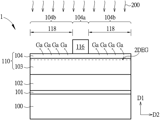
1. A method for fabricating a high-electron mobility transistor (HEMT), comprising:
providing a substrate;
forming a channel layer on the substrate;
forming an AlGaN layer on the channel layer;
forming a P—GaN gate on the AlGaN layer; and
after forming the P—GaN gate on the AlGaN layer, subjecting the AlGaN layer to a thermal treatment, thereby forming a first region comprising an entire thickness of the AlGaN layer located directly under the P—GaN gate and a second region in the AlGaN layer, wherein the second region does not overlap with the first region in a thickness direction of the AlGaN layer, wherein the first region has a composition that is different from that of the second region, and wherein a thickness of the AlGaN layer in the first region is the same as a thickness of the AlGaN layer in the second region.
|