| CPC H01L 29/42364 (2013.01) [H01L 29/42376 (2013.01); H01L 29/6656 (2013.01); H01L 29/66545 (2013.01); H01L 29/66795 (2013.01); H01L 29/785 (2013.01)] | 18 Claims |
|
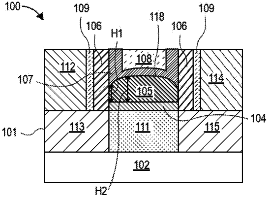
1. A semiconductor device, comprising:
a substrate;
a FinFET transistor including a fin structure on the substrate, wherein the fin structure includes a channel area, a source area, and a drain area, and the FinFET transistor includes:
a gate dielectric area between spacers, above the channel area of the fin structure, and below a top surface of the spacers, wherein the gate dielectric area has a curved surface with a first thickness closer to a spacer relative to a top surface of the fin structure and a second thickness closer to a center of the gate dielectric area relative to a top surface of the fin structure, and the first thickness is smaller than the second thickness; and
a metal gate conformally covering and in direct contact with sidewalls of the spacers, and in direct contact with the curved surface of the gate dielectric area.
|