| CPC H01L 29/4175 (2013.01) [H01L 29/66462 (2013.01); H01L 29/7786 (2013.01); H01L 29/0684 (2013.01); H01L 29/2003 (2013.01); H01L 29/205 (2013.01); H01L 29/401 (2013.01)] | 14 Claims |
|
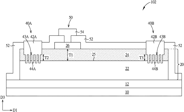
1. A high electron mobility transistor, comprising:
a substrate;
a mesa structure disposed on the substrate, wherein the mesa structure comprises a channel layer and a barrier layer on the channel layer;
a passivation layer disposed on the mesa structure;
at least a contact structure disposed in the passivation layer and the mesa structure, wherein the contact structure comprises a body portion and a plurality of protruding portions, the body portion penetrates through the passivation layer and a portion of the barrier layer, the plurality of protruding portions penetrate through the barrier layer and a portion of the channel layer, wherein a bottom surface of the body portion is lower than an upper surface of the barrier layer and higher than a bottom surface of the barrier layer; and
a gate structure disposed on the mesa structure and between the contact structure and another one of the contact structure, wherein the gate structure comprises:
a semiconductor gate layer directly disposed on the barrier layer of the mesa structure and covered by the passivation layer; and
a gate metal layer through the passivation layer to directly contact a top surface of the semiconductor gate layer.
|