| CPC H01L 29/1054 (2013.01) [H01L 29/0653 (2013.01); H01L 29/0847 (2013.01); H01L 29/66545 (2013.01); H01L 29/66553 (2013.01)] | 20 Claims |
|
1. A method comprising:
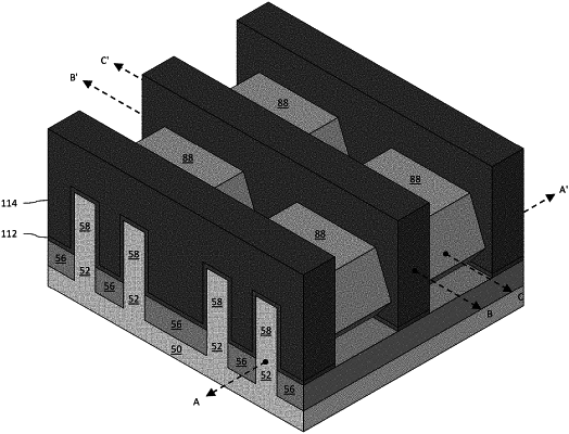
depositing an inter-layer dielectric on a source/drain region;
forming a gate mask on a gate structure, the gate structure disposed on a channel region of a substrate, the channel region adjoining the source/drain region;
implanting an impurity in the gate mask to increase an etching selectivity between the gate mask and the inter-layer dielectric relative a contact etching process; and
performing the contact etching process to pattern a contact opening in the inter-layer dielectric, the contact opening exposing the source/drain region, the gate mask covering the gate structure during the contact etching process, a protective layer being formed on the gate mask during the contact etching process, the protective layer comprising a polymer byproduct of the contact etching process.
|