US 11,695,040 B2
Self-aligned gate and drift design for high-critical field strength semiconductor power transistors with ion implantation
Kelson D Chabak, Springboro, OH (US); Andrew J Green, Beavercreek, OH (US); and Gregg H Jessen, Beavercreek, OH (US)
Assigned to United States of America as represented by the Secretary of the Air Force, Wright-Patterson AFB, OH (US)
Filed by Government of the United States, as represented by the Secretary of the Air Force, Wright-Patterson AFB, OH (US)
Filed on Mar. 24, 2021, as Appl. No. 17/210,635.
Application 17/210,635 is a division of application No. 16/869,042, filed on May 7, 2020, granted, now 11,398,551.
Claims priority of provisional application 62/844,274, filed on May 7, 2019.
Prior Publication US 2021/0234001 A1, Jul. 29, 2021
Int. Cl. H01L 29/08 (2006.01); H01L 29/417 (2006.01)
CPC H01L 29/0873 (2013.01) [H01L 29/0856 (2013.01); H01L 29/41775 (2013.01)] 22 Claims
OG exemplary drawing
 
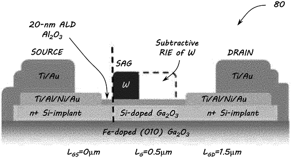
1. A method of forming a self-aligned gate (SAG) and self-aligned source (SAD) device for high Ecrit semiconductors, the method comprising:
depositing a refractory material on a high Ecrit substrate;
etching the refractory material to form a channel region;
applying an implant ionization to form a high-conductivity source region and a high-conductivity drain contact region in the high Ecrit substrate creating a self-aligned gate plus self-aligned drift feature; and
annealing to activate the source and drain contact regions,
wherein the substrate comprises an n-type Ga2O3 grown on semi-insulating Ga2O3.