| CPC H01L 29/0653 (2013.01) [H01L 21/76224 (2013.01); H01L 21/823431 (2013.01); H01L 21/845 (2013.01); H01L 27/0886 (2013.01); H01L 29/66545 (2013.01)] | 20 Claims |
|
1. A semiconductor structure, comprising:
a substrate;
a plurality of fins disposed over the substrate, at least a portion of one or more of the plurality of fins providing one or more channels for one or more fin field-effect transistors;
a plurality of active gate structures disposed over portions of the plurality of fins;
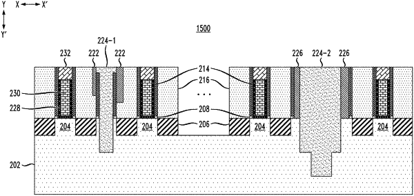
at least one single diffusion break trench between a first one of the plurality of active gate structures and a second one of the plurality of active gate structures;
at least one double diffusion break trench between a third one of the plurality of active gate structures and a fourth one of the plurality of active gate structures;
first gate sidewall spacers having first surfaces adjacent the single diffusion break trench;
a first dielectric liner disposed adjacent portions of second surfaces of the first gate sidewall spacers;
a second dielectric liner having first surfaces disposed adjacent the double diffusion break trench; and
second gate sidewall spacers adjacent second surfaces of the second dielectric liner;
wherein the double diffusion break trench has a stepped height profile in the substrate, the stepped height profile comprising a first depth with a first width and a second depth with a second width, the second depth being less than the first depth, the second width being greater than the first width.
|