| CPC H01L 29/0649 (2013.01) [H01L 27/0635 (2013.01); H01L 29/41775 (2013.01)] | 20 Claims |
|
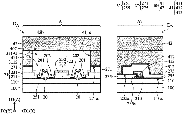
1. A semiconductor structure, comprising:
a substrate;
an active device disposed over the substrate and in a first region of the substrate;
a passive device disposed over the substrate and in a second region of the substrate; and
a passivation layer covering a top surface of the passive device, wherein the passivation layer has an opening that exposes the active device.
|