| CPC H01L 28/91 (2013.01) [H01L 27/10814 (2013.01); H01L 27/10855 (2013.01); H01L 28/92 (2013.01)] | 20 Claims |
|
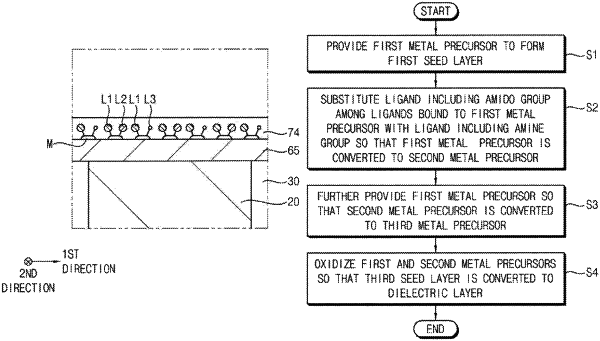
1. A method of forming a capacitor structure, the method comprising:
forming a lower electrode on a substrate;
providing a first metal precursor onto the lower electrode to form a first seed layer, the first metal precursor including a first metal and first and second ligands bound to the first metal, the first and second ligands being organic groups;
substituting the second ligand with a third ligand that has an amino group —NH2 to form a second seed layer including a second metal precursor, and wherein the amino group —NH2 of the third ligand has a size smaller than that of the amino group (—NR1R2) of the second ligand;
providing a third metal precursor onto the second seed layer to form a third seed layer, the third metal precursor including fourth and fifth ligands, and the third seed layer including the second and third metal precursors;
performing an oxidation process on the third seed layer to form a dielectric layer; and
forming an upper electrode on the dielectric layer,
wherein the dielectric layer includes a first portion and a second portion on the first portion, and wherein a detection amount of nitrogen in the dielectric layer has a maximum value at a boundary between the first portion and the second portion.
|