| CPC H01L 27/14643 (2013.01) [H01L 27/14601 (2013.01); H01L 27/14605 (2013.01); H01L 27/14683 (2013.01)] | 19 Claims |
|
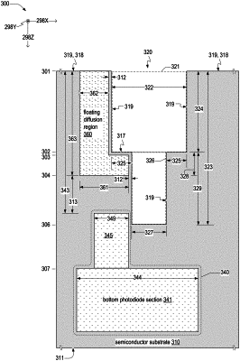
1. A method for forming a pixel comprising:
forming, in a semiconductor substrate, a wide trench having an upper depth with respect to a planar top surface of the semiconductor substrate; and
ion-implanting, between the planar top surface and a junction depth in the semiconductor substrate, a floating-diffusion region having, in a cross-sectional plane perpendicular to the planar top surface, (i) an upper width between the planar top surface and the upper depth, and (ii) between the upper depth and the junction depth, a lower width that exceeds the upper width, part of the floating-diffusion region being beneath the wide trench and between the upper depth and the junction depth.
|