| CPC H01L 27/14643 (2013.01) [H01L 27/14689 (2013.01)] | 12 Claims |
|
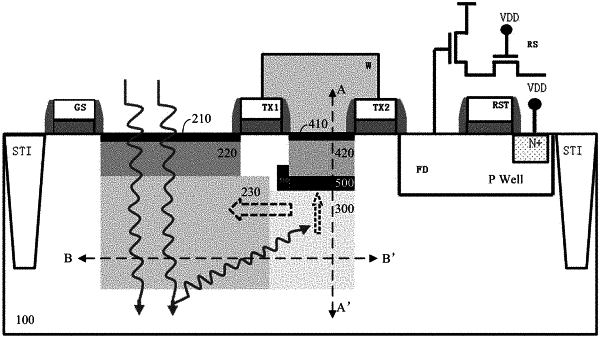
1. A semiconductor structure for forming a CMOS image sensor, the semiconductor structure comprising at least a photodiode formed in a substrate for collecting photoelectrons, wherein the photodiode has a pinning layer, a first doped region, and a second doped region in order from top to bottom in a height direction of the substrate; and
the semiconductor structure further includes a third doped region, wherein the third doped region is located in the substrate corresponding to a laterally extending region of the second doped region; wherein
the ion doping concentration of the first doped region is greater than the ion doping concentration of the second doped region, and the ion doping concentration of the second doped region is greater than the ion doping concentration of the third doped region, the third doped region is in contact with the second doped region after diffusion,
wherein the semiconductor structure further comprises a storage node formed in the substrate, and the third doped region is formed below the storage node, and
wherein the semiconductor structure further comprises a fourth doped region, and the third doped region is isolated from the storage node by the fourth doped region.
|