| CPC H01L 25/167 (2013.01) [H01L 23/5386 (2013.01); H01L 25/042 (2013.01); H01L 25/0753 (2013.01); H01L 31/02005 (2013.01); H01L 31/1892 (2013.01); H01L 33/62 (2013.01); H01L 2933/0066 (2013.01)] | 18 Claims |
|
1. An electronic device, comprising:
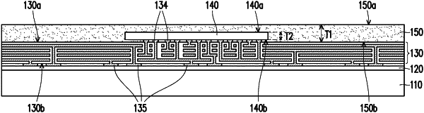
a circuit structure layer, having a first side and a second side opposite to the first side;
a package structure, disposed on the first side of the circuit structure layer and having a first thickness;
an electronic element, embedded in the package structure and having a second thickness; and
a plurality of function elements, disposed on the second side of the circuit structure layer and electrically connected to the electronic element through the circuit structure layer,
wherein the first thickness of the package structure is greater than or equal to 1.5 times the second thickness of the electronic element, and the package structure includes a single layer structure.
|