| CPC H01L 25/0657 (2013.01) [H01L 21/76831 (2013.01); H01L 21/76843 (2013.01); H01L 21/76877 (2013.01); H01L 21/76898 (2013.01); H01L 23/367 (2013.01); H01L 23/481 (2013.01); H01L 23/5226 (2013.01); H01L 23/5283 (2013.01); H01L 23/53228 (2013.01); H01L 23/53257 (2013.01); H01L 24/03 (2013.01); H01L 24/05 (2013.01); H01L 24/08 (2013.01); H01L 27/088 (2013.01); H01L 24/89 (2013.01); H01L 2224/0557 (2013.01); H01L 2224/08147 (2013.01); H01L 2224/80895 (2013.01); H01L 2224/80896 (2013.01); H01L 2225/06541 (2013.01); H01L 2225/06565 (2013.01); H01L 2225/06589 (2013.01)] | 20 Claims |
|
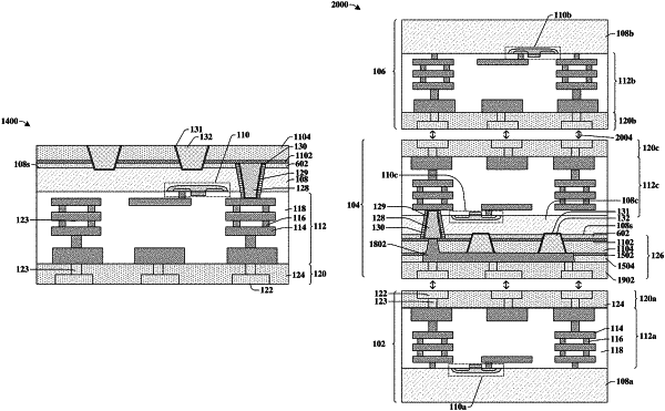
1. A method of forming an integrated circuit, the method comprising:
forming a semiconductor device on a frontside of a semiconductor substrate;
forming an interconnect structure over the semiconductor device;
forming a first bonding structure over the interconnect structure;
depositing a dielectric layer over a backside of the semiconductor substrate;
patterning the dielectric layer to form a first opening in the dielectric layer, wherein the first opening exposes a surface of the backside of the semiconductor substrate, and wherein the surface of the backside of the semiconductor substrate is above the semiconductor device when the backside of the semiconductor substrate is above the frontside of the semiconductor substrate;
depositing a glue layer having a first thickness over the first opening;
filling the first opening with a first material to form a backside contact that is separated from the semiconductor substrate by the glue layer; and
depositing more dielectric layers, bonding contacts, and bonding wire layers over the dielectric layer to form a second bonding structure on the backside of the semiconductor substrate, wherein the backside contact is coupled to the bonding contacts and the bonding wire layers.
|