| CPC H01L 25/0652 (2013.01) [H01L 21/78 (2013.01); H01L 24/08 (2013.01); H01L 24/80 (2013.01); H01L 25/18 (2013.01); H01L 25/50 (2013.01); H01L 2224/08145 (2013.01); H01L 2224/80895 (2013.01); H01L 2224/80896 (2013.01); H01L 2225/06524 (2013.01)] | 18 Claims |
|
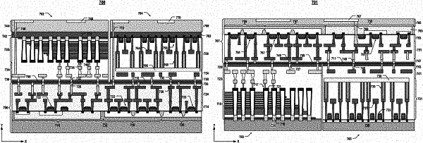
1. A semiconductor device, comprising:
a first semiconductor structure comprising an array of NAND memory cells, a first semiconductor layer above and in contact with the array of NAND memory cells, and a first bonding layer comprising a plurality of first bonding contacts, the array of NAND memory cells being above the first bonding layer;
a second semiconductor structure comprising an array of dynamic random-access memory (DRAM) cells and a second bonding layer comprising a plurality of second bonding contacts; and
a third semiconductor structure comprising a substrate, a processor on the substrate, an array of static random-access memory (SRAM) cells on the substrate and outside of the processor, and a third bonding layer above the processor and the array of SRAM cells, the third bonding layer comprising a plurality of third bonding contacts,
wherein the first bonding layer is above the third bonding layer,
the first bonding contacts are in contact with a first set of the third bonding contacts, and
the second bonding contacts are in contact with a second set of the third bonding contacts.
|