| CPC H01L 24/13 (2013.01) [H01L 22/32 (2013.01); H01L 24/06 (2013.01); H01L 24/14 (2013.01); H01L 2224/0603 (2013.01); H01L 2224/10145 (2013.01); H01L 2224/13013 (2013.01); H01L 2224/13023 (2013.01); H01L 2224/1403 (2013.01); H01L 2224/14051 (2013.01); H01L 2224/14133 (2013.01)] | 17 Claims |
|
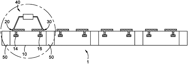
1. A test pad structure of chip, comprising:
a plurality of first internal test pads, disposed in a chip;
a plurality of second internal test pads, disposed in said chip, and spaced with said first internal test pads by a distance;
a plurality of first extended test pads, disposed on said chip, connected with said first internal test pads, and located above said first internal test pads; and
a plurality of second extended test pads, disposed on said chip, connected with said second internal test pads, and located above said second internal test pads;
wherein said first and second extended test pads transmit signals or power to said first and second internal test pads.
|