| CPC H01L 24/08 (2013.01) [H01L 21/6835 (2013.01); H01L 21/78 (2013.01); H01L 24/80 (2013.01); H01L 25/0657 (2013.01); H01L 25/50 (2013.01); H01L 2221/68327 (2013.01); H01L 2224/08145 (2013.01); H01L 2224/80006 (2013.01); H01L 2224/80895 (2013.01); H01L 2224/80896 (2013.01)] | 9 Claims |
|
1. A method of forming a semiconductor stack, comprising:
providing a carrier substrate;
disposing a plurality of first semiconductor chips that are known good dies on the carrier substrate to be horizontally spaced apart from each other;
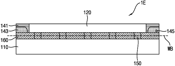
filling spaces between the first semiconductor chips with a passivation layer that contacts side surfaces of the first semiconductor chips;
forming a first layer including a plurality of first external bonding pads and a first bonding passivation layer with the first semiconductor chips, the first layer being provided on a surface of the passivation layer;
providing a plurality of second semiconductor chips horizontally adjacent to each other as part of a wafer;
providing a second layer including a plurality of second external bonding pads and a second bonding passivation layer with the second semiconductor chips;
bonding the plurality of first external bonding pads to the plurality of second external bonding pads, and bonding the first bonding passivation layer to the second bonding passivation layer to form a wafer level stacked structure; and
dicing the wafer level stacked structure to form a plurality of individual semiconductor stacks.
|