US 11,694,979 B2
Isolation structure for bond pad structure
Sin-Yao Huang, Tainan (TW); Jeng-Shyan Lin, Tainan (TW); Shih-Pei Chou, Tainan (TW); and Tzu-Hsuan Hsu, Kaohsiung (TW)
Assigned to Taiwan Semiconductor Manufacturing Company, Ltd., Hsinchu (TW)
Filed by Taiwan Semiconductor Manufacturing Co., Ltd., Hsin-Chu (TW)
Filed on Apr. 21, 2021, as Appl. No. 17/236,360.
Application 17/236,360 is a continuation of application No. 16/532,781, filed on Aug. 6, 2019, granted, now 10,991,667.
Prior Publication US 2021/0242153 A1, Aug. 5, 2021
This patent is subject to a terminal disclaimer.
Int. Cl. H01L 23/00 (2006.01); H01L 27/146 (2006.01)
CPC H01L 24/08 (2013.01) [H01L 24/03 (2013.01); H01L 27/1464 (2013.01); H01L 27/14636 (2013.01); H01L 27/14645 (2013.01); H01L 27/14689 (2013.01)] 20 Claims
OG exemplary drawing
 
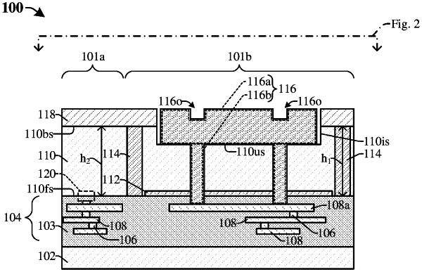
1. A method for forming a semiconductor structure, the method comprising:
forming a first isolation structure on a first surface of a substrate;
forming a second isolation structure into the first surface of the substrate, wherein sidewalls of the first isolation structure are disposed laterally between inner sidewalls of the second isolation structure; and
forming a bond pad in the substrate such that the second isolation structure continuously laterally wraps around the bond pad.