| CPC H01L 24/05 (2013.01) [H01L 24/03 (2013.01); H01L 24/11 (2013.01); H01L 24/13 (2013.01); H01L 2224/0346 (2013.01); H01L 2224/03614 (2013.01); H01L 2224/0401 (2013.01); H01L 2224/0508 (2013.01); H01L 2224/05016 (2013.01); H01L 2224/05144 (2013.01); H01L 2224/05147 (2013.01); H01L 2224/05155 (2013.01); H01L 2224/11849 (2013.01); H01L 2224/13026 (2013.01); H01L 2224/13111 (2013.01); H01L 2224/13113 (2013.01); H01L 2224/13116 (2013.01); H01L 2224/13139 (2013.01); H01L 2224/13144 (2013.01); H01L 2224/13147 (2013.01); H01L 2224/13155 (2013.01)] | 20 Claims |
|
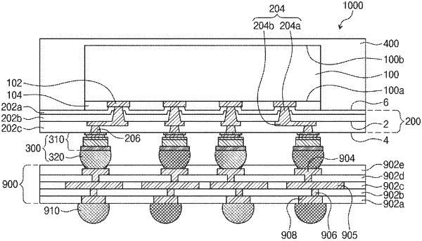
1. A semiconductor package comprising:
a first semiconductor package comprising a first re-distribution layer, a first semiconductor chip on an upper surface of the first re-distribution layer, and a terminal structure on an lower surface of the first re-distribution layer,
wherein the first re-distribution layer comprises an insulating layer and a conductive element in the insulating layer,
wherein the terminal structure comprises:
a first barrier pattern and a second barrier pattern that are sequentially stacked on a surface of the conductive element and a surface of the insulating layer;
a metal pattern on the second barrier pattern; and
a connection terminal on the metal pattern,
wherein a width of the second barrier pattern is smaller than a width of the first barrier pattern and a width of the metal pattern, and
wherein the first barrier pattern includes metal nitride.
|