| CPC H01L 23/562 (2013.01) [H01L 21/563 (2013.01); H01L 23/3157 (2013.01); H01L 24/17 (2013.01); H01L 24/32 (2013.01); H01L 24/73 (2013.01); H01L 24/81 (2013.01); H01L 24/83 (2013.01); H01L 25/0655 (2013.01); H01L 25/50 (2013.01); H01L 2224/73253 (2013.01); H01L 2924/3511 (2013.01)] | 20 Claims |
|
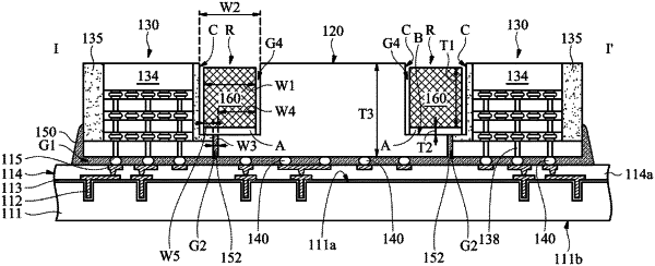
1. A chip package structure, comprising:
a substrate;
a first chip structure and a second chip structure over the substrate; and
an anti-warpage bar over a first portion of the first chip structure and over a second portion of the second chip structure, wherein a width of the anti-warpage bar overlapping the second portion of the second chip structure is greater than a width of the anti-warpage bar overlapping the first portion of the first chip structure, wherein a bottom surface of the anti-warpage bar is at a level between a top surface of the second chip structure and a bottom surface of the second chip structure.
|