| CPC H01L 23/552 (2013.01) [G06F 30/392 (2020.01); G06F 30/394 (2020.01); G06F 30/398 (2020.01); H01L 23/49822 (2013.01); H01L 23/5223 (2013.01); H01L 28/60 (2013.01); H01L 27/0207 (2013.01)] | 20 Claims |
|
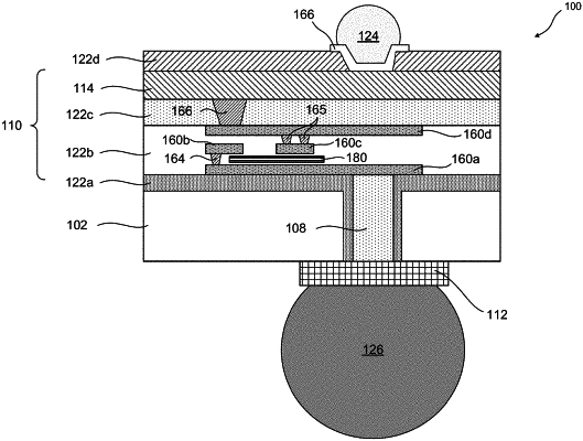
1. A semiconductor device, comprising:
a first metallization layer;
a first dielectric layer formed on the first metallization layer;
a second metallization layer formed over the first metallization layer;
a conducting line formed in the second metallization layer; and
a metal-insulator-metal (MIM) capacitor formed in the first dielectric layer and between the first and second metallization layers, the MIM capacitor comprising:
first, second, and third bottom capacitor electrodes in the first dielectric layer;
a top capacitor electrode extending above the first, second, and third bottom capacitor electrodes, wherein the top capacitor electrode is coupled to a ground voltage reference line; and
a second dielectric layer between the top electrode and the first, second, and third bottom capacitor electrodes.
|