| CPC H01L 23/552 (2013.01) [H01L 23/3675 (2013.01); H01L 23/49816 (2013.01); H01L 23/49838 (2013.01); H01L 24/16 (2013.01); H01L 24/48 (2013.01); H01L 2224/16225 (2013.01); H01L 2224/48225 (2013.01); H01L 2924/15311 (2013.01); H01L 2924/1632 (2013.01); H01L 2924/16196 (2013.01); H01L 2924/3025 (2013.01)] | 17 Claims |
|
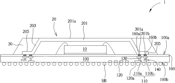
1. A semiconductor package, comprising:
a substrate;
a semiconductor die mounted on the substrate; and
a heatsink over the semiconductor die, wherein the heatsink comprises a roof portion and at least one connecting portion extending between the roof portion and the substrate, wherein the at least one connecting portion comprises a connection lead mounted on and electrically connected to a split connection pad of the substrate, wherein the split connection pad comprises a first portion and a second portion spaced apart from each other, wherein the first portion is coplanar with the second portion, and wherein the first portion is electrically connected to a first voltage signal, and the second portion is electrically connected to a second voltage signal that is different from the first voltage signal.
|