| CPC H01L 23/552 (2013.01) [H01L 21/4853 (2013.01); H01L 21/4857 (2013.01); H01L 21/565 (2013.01); H01L 23/3128 (2013.01); H01L 23/49822 (2013.01); H01L 23/49838 (2013.01); H01L 24/16 (2013.01); H01L 2224/16227 (2013.01); H01L 2924/3025 (2013.01)] | 12 Claims |
|
1. A packaged electronic device comprising:
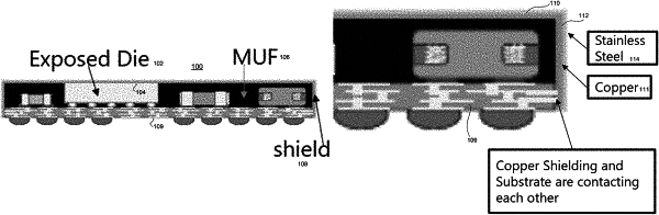
a substrate in electrical contact with a die;
a mold compound in contact with the substrate and with one or more sides of the die; and
a sputtered metal shield comprising a first layer of a first metal and a second layer of a second metal formed on the first layer, the sputtered metal shield being applied by sputtering and being in contact with the mold compound and with the substrate and extending to a bottom surface of the substrate.
|