| CPC H01L 23/544 (2013.01) [H01L 23/481 (2013.01); H01L 24/83 (2013.01); H01L 2223/54426 (2013.01); H01L 2224/8313 (2013.01)] | 10 Claims |
|
1. A semiconductor architecture comprising:
a carrier substrate;
alignment marks provided in the carrier substrate, the alignment marks being provided from a first surface of the carrier substrate to a second surface of the carrier substrate;
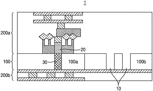
a first semiconductor device provided on the first surface of the carrier substrate based on the alignment marks, the first semiconductor device comprising a buried power rail (BPR) that is extended in a horizontal direction, and formed at an active device level different from metal interconnect structures; and
a second semiconductor device provided on the second surface of the carrier substrate based on the alignment marks and aligned with the first semiconductor device,
wherein a through-silicon via (TSV) penetrates through the carrier substrate in a vertical direction, perpendicular to the horizontal direction, and contacts the BPR and the second semiconductor device.
|