| CPC H01L 23/544 (2013.01) [H01L 21/4853 (2013.01); H01L 21/4857 (2013.01); H01L 21/565 (2013.01); H01L 21/568 (2013.01); H01L 21/78 (2013.01); H01L 23/3128 (2013.01); H01L 23/5383 (2013.01); H01L 23/5386 (2013.01); H01L 23/5389 (2013.01); H01L 24/19 (2013.01); H01L 24/20 (2013.01); H01L 2223/54426 (2013.01); H01L 2224/214 (2013.01)] | 19 Claims |
|
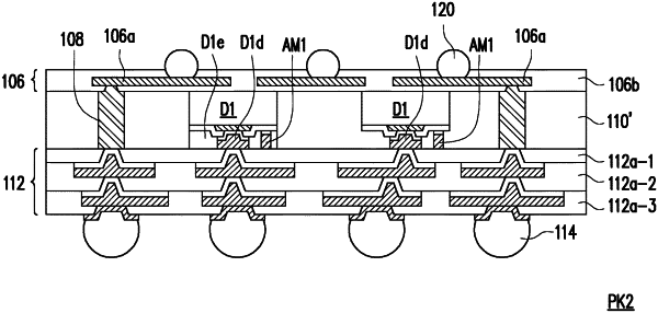
1. A package structure, comprising:
a first semiconductor die and a second semiconductor die, wherein the first semiconductor die and the second semiconductor die respectively comprises a semiconductor substrate, conductive pads disposed on the semiconductor substrate, conductive posts disposed on the conductive pads, and an alignment mark located on the semiconductor substrate, and wherein a protection layer is covering and contacting the alignment mark of the first semiconductor die;
an insulating encapsulant encapsulating the first semiconductor die and the second semiconductor die, wherein the insulating encapsulant is in physical contact with the alignment mark of the second semiconductor die, and is physically separated from the alignment mark of the first semiconductor die by the protection layer, and wherein a top surface of the insulating encapsulant is coplanar with a top surface of the conductive posts and a top surface of the alignment marks of the first semiconductor die and the second semiconductor die; and
a redistribution layer disposed on the top surface the insulating encapsulant and electrically connected to the conductive posts of the first semiconductor die and the second semiconductor die, the redistribution layer comprises:
a first dielectric layer disposed on the insulating encapsulant, covering and contacting the alignment marks of the first semiconductor die and the second semiconductor die, wherein the first dielectric layer comprises a plurality of openings revealing the top surface of the conductive posts of the first semiconductor die and the second semiconductor die;
a first seed layer disposed on and in physical contact with the first dielectric layer, wherein the first seed layer fills into the plurality of openings to be physically and electrically connected to the conductive posts of the first semiconductor die and the second semiconductor die;
a first conductive layer disposed on the first seed layer;
auxiliary alignment marks comprising an auxiliary seed layer and a conductive body disposed on the auxiliary seed layer, wherein the auxiliary alignment marks comprise a plurality of stripe patterns, and wherein a thickness of the auxiliary seed layer is equal to a thickness of the first seed layer, the first dielectric layer is physically contacting a bottom surface of the auxiliary seed layer, and a top surface of the conductive body is aligned with a top surface of the first conductive layer; and
a second dielectric layer disposed on the first dielectric layer and in physical contact with the first dielectric layer, wherein the second dielectric layer is surrounding the first seed layer, the first conductive layer and the auxiliary alignment marks, and wherein the second dielectric layer is covering and physically contacting the top surface of the conductive body and the top surface of the first conductive layer.
|