| CPC H01L 23/5222 (2013.01) [H01L 29/66462 (2013.01); H01L 29/7787 (2013.01)] | 10 Claims |
|
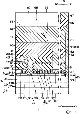
1. A semiconductor device having an electrode structure that includes a source electrode, a gate electrode, and a drain electrode disposed on a semiconductor laminated structure and extending in parallel to each other and in a predetermined first direction and a wiring structure that includes a source wiring, a drain wiring, and a gate wiring disposed on the electrode structure and extending in parallel to each other and in a second direction orthogonal to the first direction and wherein the wiring structure is one with which the source wiring, the drain wiring, and the gate wiring are electrically connected to the source electrode, the drain electrode, and the gate electrode, respectively,
the semiconductor device comprising: a conductive film disposed between the gate electrode and the drain wiring and being electrically connected to the source electrode;
wherein the conductive film extends in the first direction along an upper surface of the gate electrode,
wherein the conductive film includes a first side edge and a second side edge and the upper surface of the gate electrode includes a third side edge and a fourth side edge and wherein the first side edge corresponds to the third side edge and the second side edge corresponds to the fourth side edge, and
wherein in plan view, the first side edge projects further outward than the third side edge and the second side edge projects further outward than the fourth side edge, and wherein an amount of projection of the first side edge from the third side edge is not less than 0.3 μm and not more than 0.9 μm and an amount of projection of the second side edge from the fourth side edge is not less than 0.3 μm and not more than 0.9 μm.
|