| CPC H01L 23/49816 (2013.01) [H01L 21/486 (2013.01); H01L 21/4853 (2013.01); H01L 23/4855 (2013.01); H01L 23/49827 (2013.01); H01L 23/49838 (2013.01); H01L 23/5386 (2013.01); H01L 24/33 (2013.01)] | 21 Claims |
|
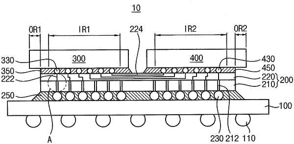
1. A semiconductor package comprising:
a package substrate;
an interposer on the package substrate, the interposer including
a semiconductor substrate, and
a wiring layer on the semiconductor substrate and including a plurality of wiring lines;
a first semiconductor device and a second semiconductor device on the interposer, the first and second semiconductor devices connected to each other by the interposer;
a first adhesive between the first semiconductor device and the interposer, the first adhesive including a first epoxy material; and
a second adhesive between the second semiconductor device and the interposer, the second adhesive including a second epoxy material,
wherein the first adhesive and the second adhesive are separated by a gap,
wherein the first semiconductor device includes an overhang portion protruding from a sidewall of the first adhesive,
wherein there is a gap between at least a portion of a bottom surface of the overhang portion and an adhesive below the overhang portion, and
wherein there are no conductive bumps beyond the sidewall of the first adhesive, under the overhang portion of the first semiconductor device, that electrically connect the first semiconductor device and the package substrate to each other.
|