| CPC H01L 23/49555 (2013.01) [H01L 21/56 (2013.01); H01L 23/3107 (2013.01); H01L 23/4951 (2013.01); H01L 23/4952 (2013.01); H01L 23/49524 (2013.01); H01L 23/49541 (2013.01); H01L 23/49551 (2013.01); H01L 23/49575 (2013.01); H01L 24/14 (2013.01); H01L 24/17 (2013.01); H01L 24/29 (2013.01); H01L 24/32 (2013.01); H01L 24/81 (2013.01); H01L 24/83 (2013.01); H01L 25/0657 (2013.01); H01L 25/072 (2013.01)] | 27 Claims |
|
1. A semiconductor device, comprising:
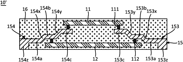
a substrate comprising leads, the leads comprising:
lead terminals;
lead steps; and
lead offsets extending between the lead steps so that at least some lead steps reside on different planes;
a first electronic component coupled to a first lead step side, the first electronic component comprising:
a first electronic component first side comprising a first active side; and
a first electronic component second side opposite to the first electronic component first side;
a second electronic component coupled to a second lead step side, the second electronic component comprising:
a second electronic component first side comprising a second active side; and
a second electronic component second side opposite to the second electronic component first side;
conductive bumps comprising a first conductive bump and a second conductive bump; and
an encapsulant encapsulating the first electronic component, the second electronic component, the first conductive bump, the second conductive bump, and portions of the substrate,
wherein:
the first active side faces and is connected to the first lead step side with the first conductive bump;
the second active side faces and is connected to the second lead step side with the second conductive bump;
the lead terminals are exposed from a first side of the encapsulant;
the first electronic component second side is exposed from a second side of the encapsulant; and
the second side of the encapsulant is different than the first side of the encapsulant.
|