| CPC H01L 23/473 (2013.01) [H01L 21/4857 (2013.01); H01L 21/4882 (2013.01); H01L 21/568 (2013.01); H01L 21/6835 (2013.01); H01L 23/3121 (2013.01); H01L 23/4006 (2013.01); H01L 24/19 (2013.01); H01L 24/20 (2013.01); H01L 2023/4018 (2013.01); H01L 2023/4068 (2013.01); H01L 2023/4087 (2013.01); H01L 2221/68359 (2013.01)] | 20 Claims |
|
1. A semiconductor device, comprising:
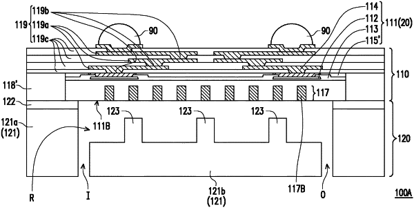
a chip package comprising a semiconductor die laterally encapsulated by an insulating encapsulant, the semiconductor die comprising a thermal enhancement pattern; and
a heat dissipation structure connected to the chip package, the heat dissipation structure comprising a heat spreader comprising a flow channel and a cooling liquid in the flow channel, and the cooling liquid in the flow channel being in contact with the thermal enhancement pattern, wherein outer sidewalls of the heat spreader are substantially aligned with outer sidewalls of the insulating encapsulant.
|