| CPC H01L 21/823864 (2013.01) [H01L 21/823821 (2013.01); H01L 21/823878 (2013.01); H01L 27/0924 (2013.01); H01L 29/66545 (2013.01); H01L 29/66795 (2013.01); H01L 29/785 (2013.01)] | 20 Claims |
|
1. A semiconductor structure, comprising:
a fin disposed over a substrate;
an isolation region disposed adjacent to the fin;
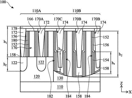
a first metal gate structure disposed over the fin, wherein a portion of the first metal gate structure along a lengthwise direction of the fin extends entirely over a top surface of the fin;
source/drain (S/D) features disposed over the fin and adjacent to the first metal gate structure;
a second metal gate structure, wherein, in a cross-sectional view cut through the fin and the isolation region, an entirety of the second metal gate structure is disposed directly over the isolation region and is not vertically overlapped with the fin;
a gate spacer disposed on a bottom portion of sidewalls of the second metal gate structure, wherein a top portion disposed above the bottom portion of the sidewalls of the second metal gate structure is free of the gate spacer;
a first dielectric layer disposed on sidewalls of the first metal gate structure and on the sidewalls of the second metal gate structure, wherein the first dielectric layer is separated from the sidewalls of the first metal gate structure by an air gap but directly contacts the top portion of the sidewalls of the second metal gate structure;
a second dielectric layer disposed over the first metal gate structure and the first dielectric layer; and
S/D contacts disposed over the S/D features.
|