| CPC H01L 21/823475 (2013.01) [H01L 21/76802 (2013.01); H01L 21/76877 (2013.01); H01L 21/76897 (2013.01); H01L 21/823431 (2013.01); H01L 23/485 (2013.01); H01L 23/5226 (2013.01); H01L 27/0886 (2013.01); H01L 29/0642 (2013.01); H01L 29/0649 (2013.01); H01L 29/41791 (2013.01); H01L 29/66795 (2013.01); H01L 29/785 (2013.01); H01L 21/823481 (2013.01)] | 20 Claims |
|
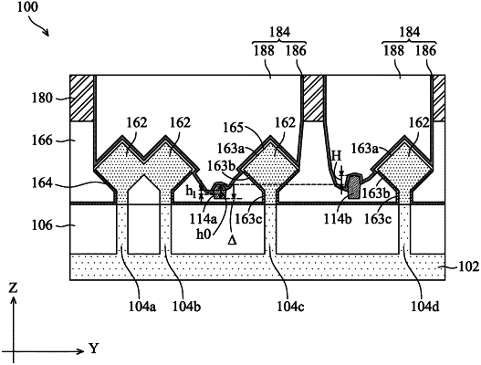
1. A semiconductor device, comprising:
a substrate;
first and second fins protruding from the substrate;
first and second source/drain (S/D) features over the first and second fins respectively;
an isolation feature over the substrate and disposed between the first and second S/D features; and
a dielectric layer disposed on sidewalls of the first and second S/D features and on sidewalls of the isolation feature,
wherein a top portion of the isolation feature extends above the dielectric layer, and wherein the top portion of the isolation feature is below the first and second S/D features.
|