| CPC H01L 21/76897 (2013.01) [H01L 21/76805 (2013.01); H01L 21/76895 (2013.01); H01L 23/5283 (2013.01); H01L 23/535 (2013.01); H01L 29/0653 (2013.01); H01L 29/0847 (2013.01); H01L 29/66795 (2013.01); H01L 29/7848 (2013.01); H01L 29/7851 (2013.01)] | 20 Claims |
|
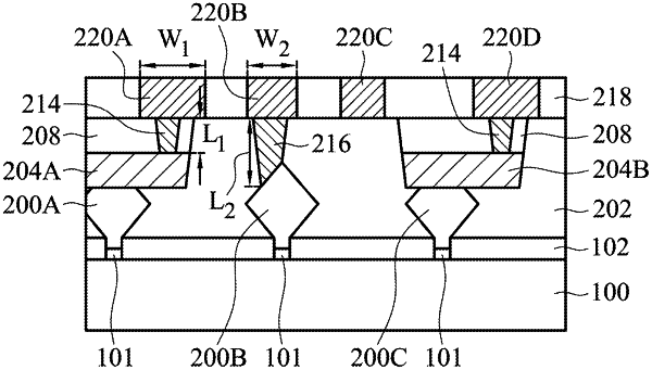
1. A method for forming a semiconductor device structure, comprising:
forming a first source/drain structure and a second source/drain structure over a semiconductor substrate;
forming a dielectric layer over the first source/drain structure and the second source/drain structure;
forming a conductive contact on the first source/drain structure;
forming a first conductive via over the conductive contact, wherein the first conductive via is misaligned with the first source/drain structure; and
forming a second conductive via directly above the second source/drain structure, wherein the second conductive via is longer than the first conductive via.
|