| CPC H01L 21/76844 (2013.01) [H01L 21/7684 (2013.01); H01L 21/76805 (2013.01); H01L 21/76834 (2013.01); H01L 21/76846 (2013.01); H01L 21/76849 (2013.01); H01L 21/76895 (2013.01); H01L 23/535 (2013.01)] | 20 Claims |
|
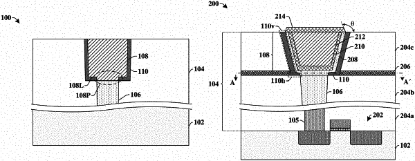
1. An integrated chip, comprising:
a first interconnect disposed between lower sidewalls of an inter-level dielectric (ILD) structure over a substrate, the first interconnect having sidewalls that contact the lower sidewalls of the ILD structure along interfaces as viewed along a cross-sectional view;
a barrier layer disposed along upper sidewalls of the ILD structure and having sidewalls defining an opening over the first interconnect;
a second interconnect disposed on the barrier layer, wherein the second interconnect extends through the opening in the barrier layer and to the first interconnect and wherein a bottommost surface of the barrier layer laterally extends past an interior sidewall of the barrier layer that faces the second interconnect; and
wherein opposing outermost edges of a bottommost surface of the second interconnect are laterally aligned with the interfaces.
|