| CPC H01L 21/7682 (2013.01) [H01L 21/76885 (2013.01); H01L 23/528 (2013.01); H01L 23/5226 (2013.01); H01L 23/5329 (2013.01)] | 9 Claims |
|
1. A method for preparing a semiconductor device, comprising:
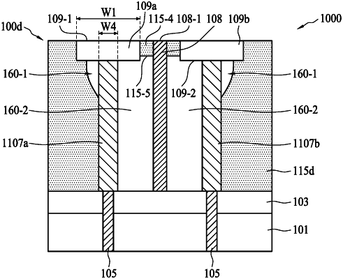
forming a plurality of composite pillars over a substrate, wherein the composite pillars include conductive pillars and dielectric caps over the conductive pillars;
transforming a sidewall portion of the conductive pillar into a first transformed portion;
removing the first transformed portion such that a width of the dielectric cap is greater than a width of a remaining portion of the conductive pillar;
forming a supporting pillar between adjacent two of the plurality of composite pillars; and
forming a sealing layer at least contacts a top portion of the supporting pillar and a top of the dielectric cap, and air spacers are formed between the sealing layer, the supporting pillar and the remaining portions of the conductive pillars;
wherein the sealing layer has an intervening portion contacting the top portion of the supporting pillar and the top portion of the dielectric cap, and the intervening portion has a bottom end lower than a bottom end of the dielectric cap.
|