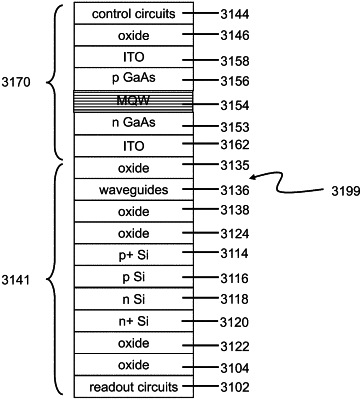
Multilevel semiconductor device and structure with oxide bonding
Zvi Or-Bach, Haifa (IL); Deepak C. Sekar, Sunnyvale, CA (US); and Brian Cronquist, Klamath Falls, OR (US)
Assigned to Monolithic 3D Inc., Klamath Falls, OR (US)
Filed by Monolithic 3D Inc., Klamath Falls, OR (US)
Filed on Jan. 28, 2023, as Appl. No. 18/102,710.
Application 18/102,710 is a continuation in part of application No. 17/868,776, filed on Jul. 20, 2022, granted, now 11,594,526.
Application 17/868,776 is a continuation in part of application No. 17/717,094, filed on Apr. 10, 2022, granted, now 11,437,368, issued on Sep. 6, 2022.
Application 17/717,094 is a continuation in part of application No. 17/492,627, filed on Oct. 3, 2021, granted, now 11,327,227, issued on May 10, 2022.
Application 17/492,627 is a continuation in part of application No. 17/330,186, filed on May 25, 2021, granted, now 11,163,112, issued on Nov. 2, 2021.
Application 17/330,186 is a continuation in part of application No. 17/189,201, filed on Mar. 1, 2021, granted, now 11,063,071, issued on Jul. 13, 2021.
Application 17/189,201 is a continuation in part of application No. 17/121,726, filed on Dec. 14, 2020, granted, now 10,978,501, issued on Apr. 13, 2021.
Application 17/121,726 is a continuation in part of application No. 17/027,217, filed on Sep. 21, 2020, granted, now 10,943,934, issued on Mar. 9, 2021.
Application 17/027,217 is a continuation in part of application No. 16/860,027, filed on Apr. 27, 2020, granted, now 10,833,108, issued on Nov. 10, 2020.
Application 16/860,027 is a continuation in part of application No. 15/920,499, filed on Mar. 14, 2018, granted, now 10,679,977, issued on Jun. 9, 2020.
Application 15/920,499 is a continuation in part of application No. 14/936,657, filed on Nov. 9, 2015, granted, now 9,941,319, issued on Apr. 10, 2018.
Application 14/936,657 is a continuation in part of application No. 13/274,161, filed on Oct. 14, 2011, granted, now 9,197,804, issued on Nov. 24, 2015.
Application 13/274,161 is a continuation in part of application No. 12/904,103, filed on Oct. 13, 2010, granted, now 8,163,581, issued on Apr. 24, 2012.
Prior Publication US 2023/0170250 A1, Jun. 1, 2023